Prof. Hogg, CTO at III-V Epi Ltd, explains how epitaxial regrowth enhances semiconductor laser performance
20 December 2023
Professor Richard Hogg, Chief Technical Officer at III-V Epi, explains how design engineers might use epitaxial regrowth to enhance semiconductor laser performance and unlock new markets.
First, Richard looks at the relatively mature, epitaxial regrowth process for indium phosphide (InP) lasers, commonly used in 5G, datacoms, telecoms and co-located optics applications. Richard then considers gallium arsenide (GaAs), a less mature material system, which suits a multitude of emerging, laser applications in industrial, biomedical imaging, datacomms, and sensing. Epitaxial regrowth better meets the need for greater heat dissipation; reduced optical loss; and the ever-increasing demand for photonics integration. It also brings the next-generation, device performance necessary for semiconductor lasers of the future.
Current InP device manufacturing technologies involve multiple epitaxy (additive) and fabrication steps (lithography and subtractive etch) to form the semiconductor laser. These technologies contrast with the more basic ridge-laser structures, where one epitaxy step is followed by subtractive etching to form a waveguide, with passivation and isolation to produce electrical contacts. Figure 1.
For InP devices, these epitaxial regrowth processes enable a range of photonic integrated circuit (PIC) building blocks to be produced, such as low loss DFB and DBR sections; gain and passive sections; and buried heterostructures for low optical loss and enhanced heat extraction. InP material systems operate in the 1200-1700nm range, whereas GaAs material systems range from red, 650nm quantum wells, to near infra-red (NIR), 1300nm quantum dots (QDs). This wide range enables new applications in optical datacomms, silicon photonics, biomedical imaging, displays, data storage, and much more. Epitaxial regrowth processes for GaAs are immature in comparison to InP, however, to realise next-generation devices, it is critically important that performance is extended beyond that of current epitaxy and ridge waveguide technologies.
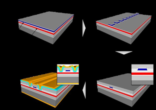
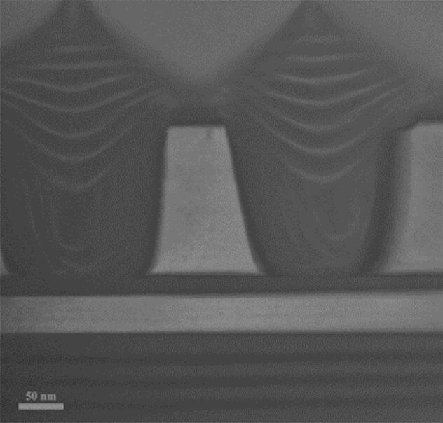
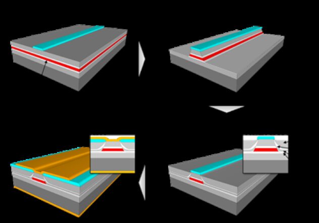
Distributed feedback (DFB) lasers are typical of a device manufactured by epitaxial regrowth, Figure 2. Initially, the lower cladding and active elements (quantum wells) of the laser are epitaxially grown on a substrate. After cleaning and etching, a grating structure is formed in the wafer substrate surface, using electron beam lithography, and etching, to give the distributed feedback (DFB), laser mechanism. This produces the correct period and depth of grating for the optical properties required.
Epitaxial regrowth is usually performed by a metal-organic, chemical, vapor deposition (MOCVD) machine, which deposits semiconductor layers onto the substrate surface and grating. A cladding and cap layer ‘sandwich’ the active region with the DFB grating of the laser. This provides optical confinement and guides the light, which is emitted from the lasers facet.
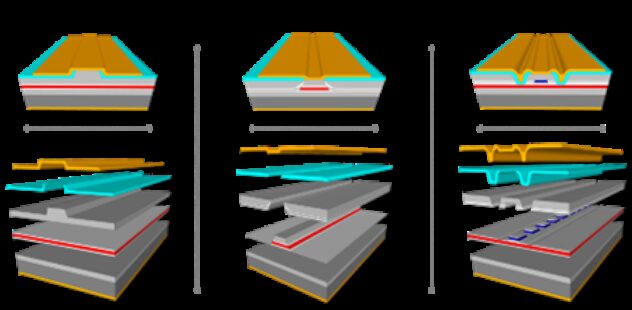
Within the process, a range of parameters are controlled, such as temperature, supply of reagents and pressure, to achieve the correct material properties, crystalline quality, and uniformity across the wafer. Dopants can also be introduced to ensure the required conductivity. From here the wafer may be processed into an individual laser die, in the form of a ridge waveguide laser. Alternatively, the wafer may proceed through other epitaxial regrowth steps to make a buried heterostructure, as shown in Figure 3. Here, optical confinement is much gentler than for a ridge laser, and current confinement is achieved through either a blocking p-n-p-n structure, or making the overgrown material semi-insulating, such as through doping with iron.
Buried heterostructures allow improved heat extraction and hence greater output power. They also allow more symmetrical output beams, resulting in lower power loss in the subsequent optical systems and reducing the costs to fibre-package.
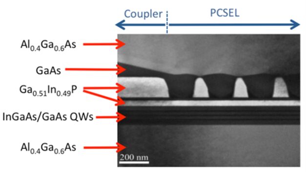
III-V Epi develops epitaxial regrowth processes for InP and GaAs materials. The company has developed know-how in the re-growth of GaAs-based components over several years, employing the use of “marker” layers to track the re-growth front, Figure 4. Not only does this allow novel, GaAs-based, PIC devices to be produced, Figure 5, but it also has capabilities for in-situ etching (cleaning) of the wafer and doping of regrown materials to enable current blocking layers, such as iron doped indium phosphide lasers (InP:Fe).